This session covers the two main classes of disordered and partly ordered materials, and the workshop will take an audience vote on which hands-on demo to run: polymer flowline mapping or the pair distribution function of an amorphous metal. Both notebooks are linked above, so you can run the other one at home.
Semicrystalline polymers
Semicrystalline polymers and small-molecule organic films (conjugated polymers for organic electronics, polyolefins, peptide and protein assemblies) derive their properties from nanoscale crystalline domains embedded in an amorphous matrix. Charge transport in an organic semiconductor, for example, depends on how the π-stacking direction of crystallites connects across the film. These materials are essentially impossible to characterize by conventional high-resolution imaging: they are extremely beam sensitive, with critical fluences of order 1–100 e⁻/Ų, destroyed long before an atomic-resolution image can be formed Bustillo et al. (2021).
Nanobeam 4D-STEM sidesteps this. Diffraction concentrates the structural information from the whole illuminated volume into a few sharp features, so a useful diffraction pattern can be recorded with orders of magnitude fewer electrons than an image Panova et al. (2016), and with a fast camera, the dose is spread over the full field of view in a single low-fluence pass.
From diffraction patterns to orientation maps
Polymer crystallites typically produce a strong, characteristic reflection (e.g., the ~3.6 Å π–π stacking peak in P3HT, or lamellar/backbone reflections at lower angles). Because of local disorder, these appear as azimuthal arcs rather than sharp spots:
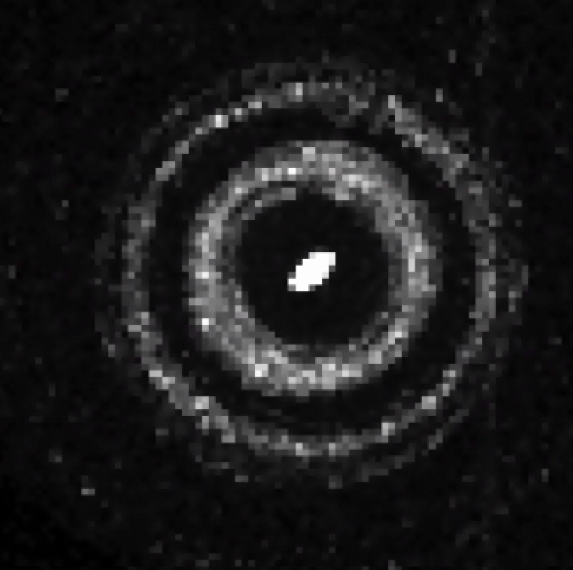
A single nanobeam pattern from a semicrystalline polymer: the characteristic reflections appear as azimuthal arcs whose angular position encodes the local crystallite orientation.
The workflow:
Detect the arcs. At each probe position, locate the azimuthal position of the characteristic reflection. Polar transformation of each pattern makes the azimuthal intensity distribution easy to fit, and peak prominence (rather than absolute intensity) is the robust detection criterion for weak, diffuse signal.
Map orientation. The azimuthal angle of the arc gives the local crystallite orientation (modulo the symmetry of the reflection); its intensity gives the degree of crystallinity/alignment. The result is an orientation field over the scanned area.
Draw flowlines. Orientation fields are hard to read as color maps alone. Flowline maps Panova et al. (2019), streamlines integrated through the orientation vector field drawn with density proportional to local alignment, render the connectivity of the crystalline regions directly, in images reminiscent of van Gogh’s Starry Night:
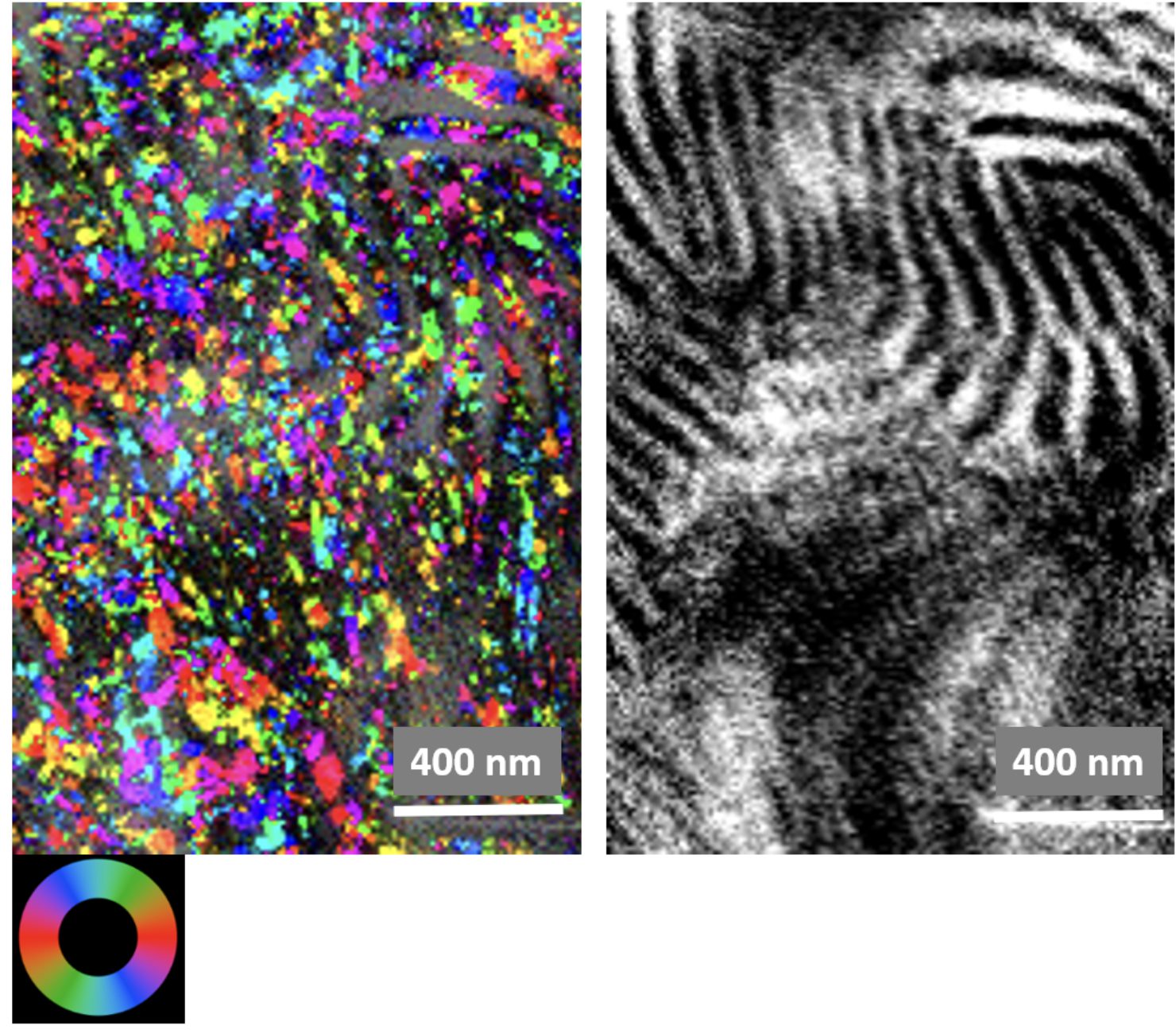
From orientation field to flowlines: the same region shown as an orientation color map (left) and as a flowline map (right). Connectivity, domain size, and topological defects in the orientation field become immediately readable.
Dose-limited experiment design
Everything about these experiments is a dose budget negotiation:
Total fluence must stay below the damage threshold; measure the critical dose for your material first (e.g., by watching a reflection fade under repeated exposure).
Step size vs. probe size: large scan steps (often ≫ probe size) spread the dose; the orientation field is smooth enough that sparse sampling still captures it.
Cryo helps: cooling typically increases critical dose by a factor of a few.
Detector: electron counting and high frame rates let you work at the shot-noise limit; pattern-level denoising and radial-symmetry priors can be applied in analysis.
Amorphous materials and pair distribution functions
Glasses, amorphous thin films, liquids, and highly disordered solids have no unit cell, so the crystallographic toolkit of the morning sessions (Bragg disks, lattice vectors, orientation libraries) does not apply. But these materials are far from structureless: they have well-defined bond lengths, coordination shells, and often medium-range order (MRO) extending over 1–3 nm. This module covers how to quantify that structure from nanobeam diffraction Cockayne (2007).
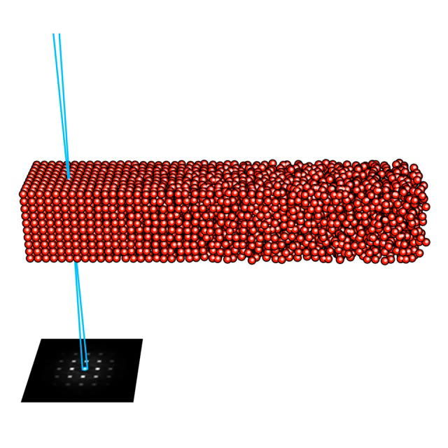
Crystalline order produces sharp Bragg spots; amorphous structure produces diffuse rings. The rings still encode quantitative structural information (bond lengths and coordination shells), which the pair distribution function extracts.
Describing disorder: n-body distribution functions
Without a lattice, structure is described statistically. The workhorse is the two-body pair distribution function g(r): the probability, relative to a random ideal gas, of finding an atom at distance r from another atom. Sharp peaks at the nearest-neighbor distance and progressively broader peaks at higher shells encode the local bonding; how quickly the oscillations decay measures the extent of order:
A nanocrystalline material shows sharp, persistent peaks out to large r.
A material with medium-range order shows a sharp first shell and damped oscillations that die out over a few nanometers.
A liquid or fully amorphous structure shows a sharp minimum bond distance, a strong first shell, and essentially no structure beyond the second or third shell.
For multi-component systems the bookkeeping multiplies: two elements A and B produce three partial PDFs (A–A, B–B, A–B).
Measuring the PDF with electron diffraction (ePDF)
Diffraction measures the Fourier transform of g(r). From a 4D-STEM dataset of an amorphous sample the workflow is:
Polar transform. Convert each diffraction pattern from Cartesian (kx, ky) to polar (φ, k) coordinates. This step is exquisitely sensitive to the pattern origin: an incorrect center produces wavy azimuthal artifacts that corrupt everything downstream. Automatic origin refinement (minimizing the standard deviation of intensity along the azimuthal direction at each probe position) makes this robust at scale.
Azimuthal average → I(k). Average over φ to get the radial scattering intensity:
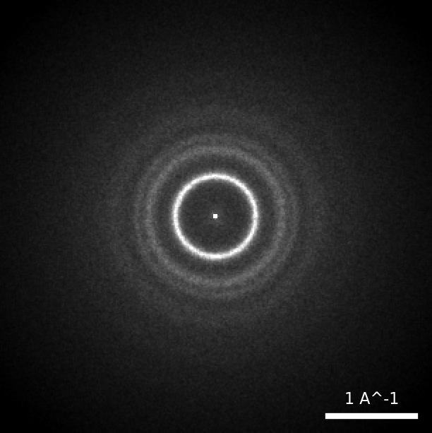
The starting point: a diffuse-ring diffraction pattern from an amorphous film. Reaching high scattering vectors (several Å⁻¹) and filtering the inelastic background both pay off directly in PDF quality.
Background subtraction. Fit and remove the smooth single-atom scattering background, e.g. with a model of the form
Reduced structure factor. Convert the background-corrected intensity to the reduced structure factor F(k) = k·(S(k) − 1).
Sine transform → G(r). A windowed sine transform of F(k) gives the reduced PDF G(r). Truncation of the k-range produces spurious low-r oscillations (atoms cannot be 0.5 Å apart!); damping schemes that iteratively fit S(k) and estimate the atomic number density ρ₀ suppress these artifacts Yoshimoto & Omote (2022).
Normalize → g(r). With the density in hand, :
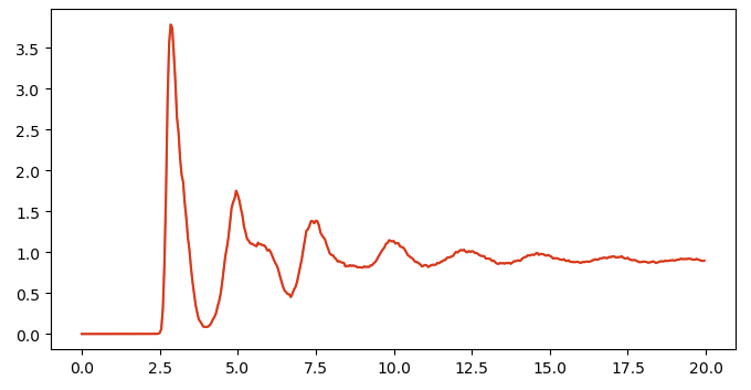
The result: g(r) with its sharp first-neighbor peak and decaying coordination-shell oscillations, the quantitative fingerprint of the local atomic structure.
Because each step has failure modes, validation matters: in the tutorial we use a simulated 4D-STEM dataset of amorphous tantalum (built on the liquid/glass models of Ding et al. (2017)), so the measured g(r) can be compared against the ground-truth PDF computed directly from the atomic coordinates.
Beyond the mean: mapping disorder in 4D
Unlike a selected-area or powder ePDF, a 4D-STEM measurement retains spatial resolution: each probe position carries its own diffuse-scattering signal, so you can map local structure:
Spatially resolved PDFs distinguish amorphous phases, map crystalline/amorphous phase fractions, and track devitrification.
Fluctuation electron microscopy (FEM): the variance of the diffracted intensity between probe positions (as a function of k and probe size) is sensitive to medium-range order that is invisible in the mean pattern Treacy et al. (2005), Voyles & Muller (2002):
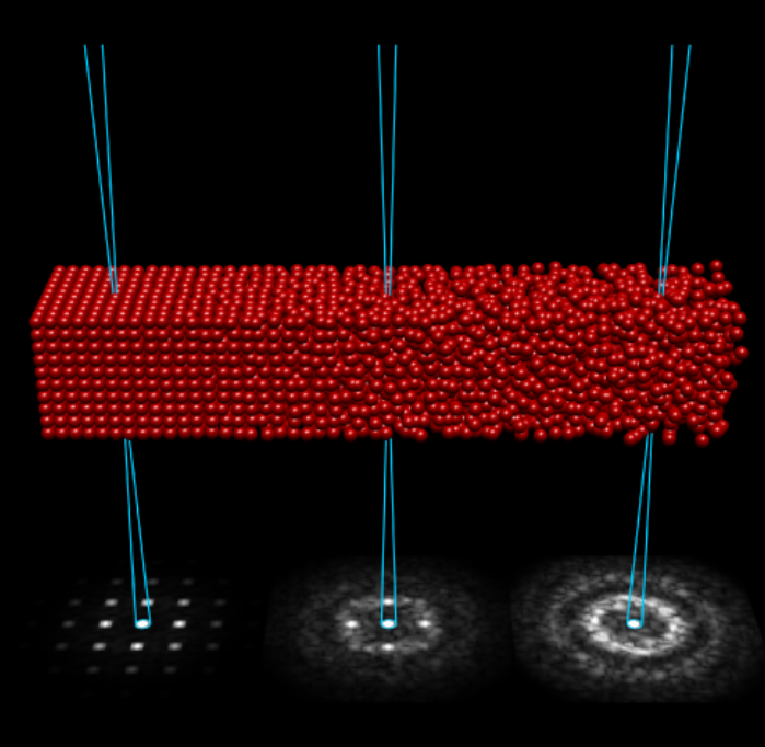
Fluctuation electron microscopy: as the probe moves across a disordered sample, the diffuse speckle changes from position to position. The variance of the intensity between positions measures medium-range order that the mean pattern averages away.
Elliptic distortions of the amorphous halo are a signal, not just a nuisance: under mechanical load, the halo of a metallic glass distorts measurably, so fitting ellipses to the rings maps strain in amorphous materials, extending the morning’s strain-mapping ideas to samples with no lattice at all:
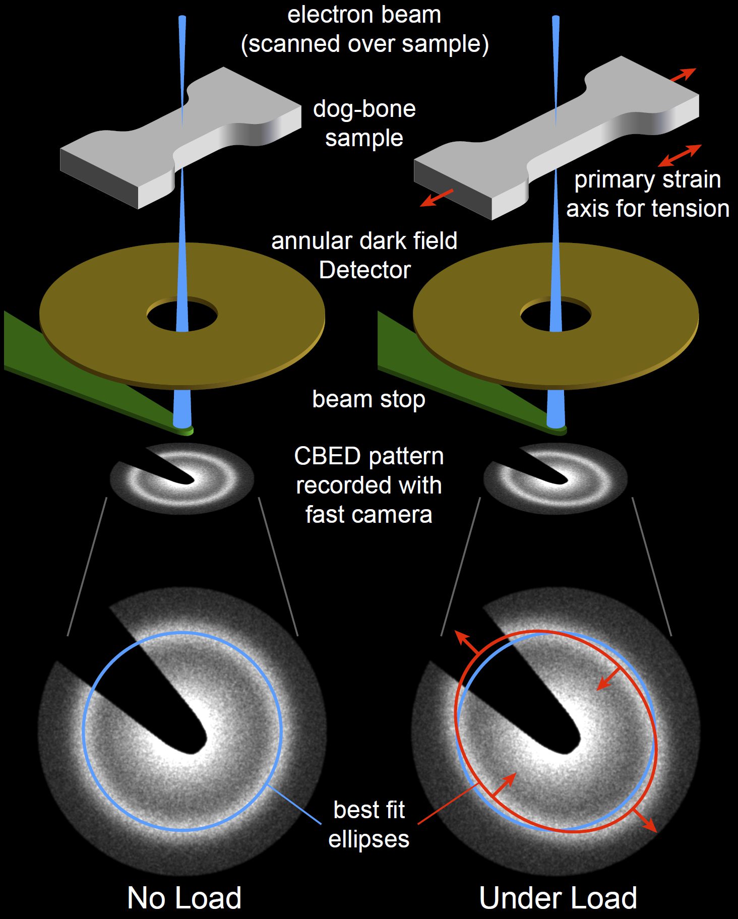
Strain mapping without a lattice: in-situ tension on a dog-bone metallic glass sample. Under load, the amorphous ring becomes measurably elliptical, and the fitted ellipse parameters give the local strain tensor.
Practical notes
Reach high enough k (several Å⁻¹): camera length down, and mind the detector corners.
Energy filtering removes the inelastic background and markedly improves S(k) at low k.
Amorphous halos also calibrate elliptical distortion for all the crystalline analyses; see the data handling module.
- Bustillo, K. C., Zeltmann, S. E., Chen, M., Donohue, J., Ciston, J., Ophus, C., & Minor, A. M. (2021). 4D-STEM of Beam-Sensitive Materials. Accounts of Chemical Research, 54(11), 2543–2551. 10.1021/acs.accounts.1c00073
- Panova, O., Chen, X. C., Bustillo, K. C., Ophus, C., Bhatt, M. P., Balsara, N., & Minor, A. M. (2016). Orientation mapping of semicrystalline polymers using scanning electron nanobeam diffraction. Micron, 88, 30–36. 10.1016/j.micron.2016.05.008
- Panova, O., Ophus, C., Takacs, C. J., Bustillo, K. C., Balhorn, L., Salleo, A., Balsara, N., & Minor, A. M. (2019). Diffraction imaging of nanocrystalline structures in organic semiconductor molecular thin films. Nature Materials, 18(8), 860–865. 10.1038/s41563-019-0387-3
- Cockayne, D. J. H. (2007). The Study of Nanovolumes of Amorphous Materials Using Electron Scattering. Annual Review of Materials Research, 37(1), 159–187. 10.1146/annurev.matsci.35.082803.103337
- Yoshimoto, M., & Omote, K. (2022). Determination of Atomic-Scale Density of Materials from Total Scattering Profiles. Journal of the Physical Society of Japan, 91(10). 10.7566/jpsj.91.104602
- Ding, J., Asta, M., & Ritchie, R. O. (2017). On the question of fractal packing structure in metallic glasses. Proceedings of the National Academy of Sciences, 114(32), 8458–8463. 10.1073/pnas.1705723114
- Treacy, M. M. J., Gibson, J. M., Fan, L., Paterson, D. J., & McNulty, I. (2005). Fluctuation microscopy: a probe of medium range order. Reports on Progress in Physics, 68(12), 2899–2944. 10.1088/0034-4885/68/12/r06
- Voyles, P. M., & Muller, D. A. (2002). Fluctuation microscopy in the STEM. Ultramicroscopy, 93(2), 147–159. 10.1016/s0304-3991(02)00155-9