In four-dimensional scanning transmission electron microscopy (4D-STEM), we scan a focused or nearly-parallel electron probe over a two-dimensional grid of positions on the sample, and record a full two-dimensional diffraction pattern at every position Ophus (2019). The result is a four-dimensional dataset: two real-space scan dimensions and two reciprocal-space detector dimensions.
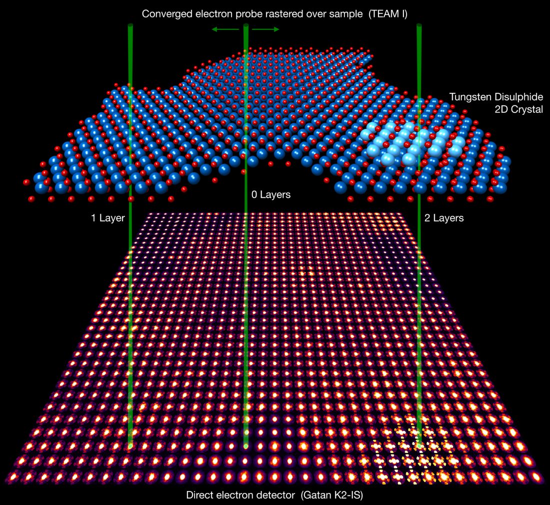
A 4D-STEM experiment: a converged probe is rastered over the sample (here a WS₂ monolayer with islands of additional layers), and a full diffraction pattern is recorded at every probe position.
Almost every analysis in this course (strain mapping, orientation mapping, virtual imaging, polymer orientation, pair distribution functions) starts from the same kind of measurement, and the quality of every one of them is set at the microscope, before any software is involved. Where conventional STEM integrates each pattern down to one number per detector per position, 4D-STEM keeps everything:
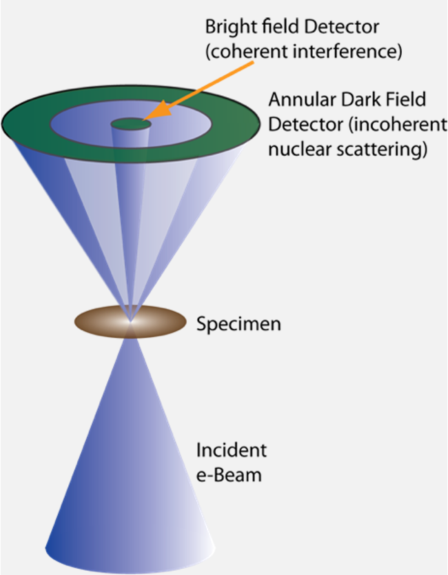
Conventional STEM integrates the scattered signal on monolithic bright field and annular dark field detectors. A 4D-STEM camera replaces (or supplements) these with a full image of the diffraction plane.
The fundamental trade-off: probe size vs. angular resolution
The convergence semi-angle α of the probe controls both the real-space probe size and the size of the diffracted Bragg disks. A large convergence angle gives a small probe (better spatial resolution) but large, potentially overlapping disks; a small convergence angle gives sharp, well-separated diffraction spots but a wider probe. Disk overlap begins when 2α exceeds the Bragg angle separation of adjacent reflections, so for disk-registration methods such as strain mapping we typically choose α from a fraction of a milliradian up to a few milliradians: the “nanobeam” regime, with probe sizes of roughly 1–5 nm.
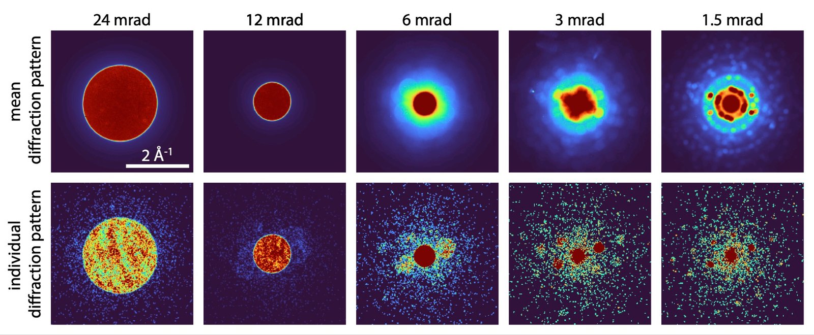
Mean (top) and single (bottom) diffraction patterns as the convergence semi-angle is stepped from 24 mrad down to 1.5 mrad: large angles overlap the disks into an interference-rich pattern, small angles give sharp, well-separated nanobeam spots.
Things to consider when choosing probe conditions:
Convergence angle: small enough that disks of interest do not overlap, large enough that the probe stays small compared to the microstructural features you want to resolve. Disk-edge sharpness also sets how precisely disk positions can be measured.
Probe current and dose: disk registration works well even at low dose, but weak reflections (superlattice peaks, high-order Laue zones, amorphous halos) need adequate counts. For beam-sensitive materials (see the polymer module), total fluence budgets of 1–100 e⁻/Ų may apply Bustillo et al. (2021), which dictates probe current, dwell time, and step size.
Scan step size: for mapping, the step is usually chosen comparable to or larger than the probe size. Oversampling wastes dose; undersampling misses microstructure.
Camera length: sets which scattering angles land on the detector. Strain and orientation mapping want the first few orders of Bragg reflections; PDF measurements want to reach high scattering vectors (several Å⁻¹).
Aperture size: the physical condenser aperture sets the convergence angle and the coherence of the illumination, and smaller apertures can substantially improve the signal-to-noise of weak reflections by sharpening the diffracted spots:
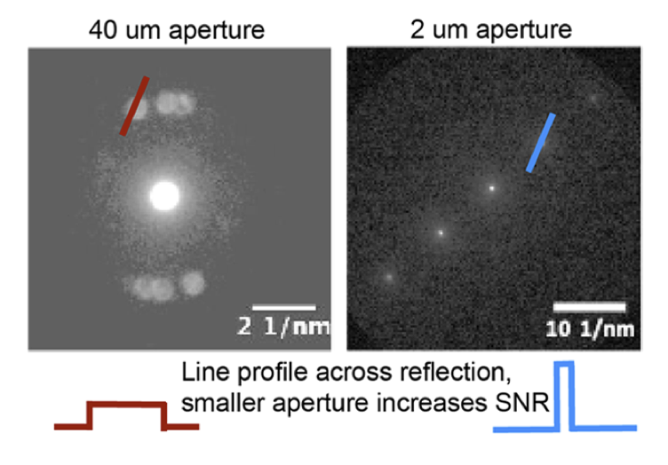
Aperture choice in practice: stepping from a 40 μm to a 2 μm condenser aperture sharpens the reflections, increasing the peak signal-to-noise for the same total dose.
Detectors and cameras
Modern 4D-STEM is enabled by fast direct electron detectors Nord et al. (2020). Relevant camera parameters:
Frame rate sets the total acquisition time: a 512×512 real-space scan at 1 kHz takes over four minutes, long enough that sample drift and contamination matter. Modern detectors run from ~1 kHz (hybrid pixel array detectors Tate et al. (2016)) up to ~100 kHz (thin active pixel sensors).
Dynamic range: the unscattered central beam can be 10⁴–10⁶ times more intense than the weakest features of interest. High-dynamic-range detectors, a beamstop, or patterned apertures prevent saturation.
Detector counts and noise: electron-counting detectors give Poisson-limited data, which is what makes low-dose diffraction analysis quantitative.
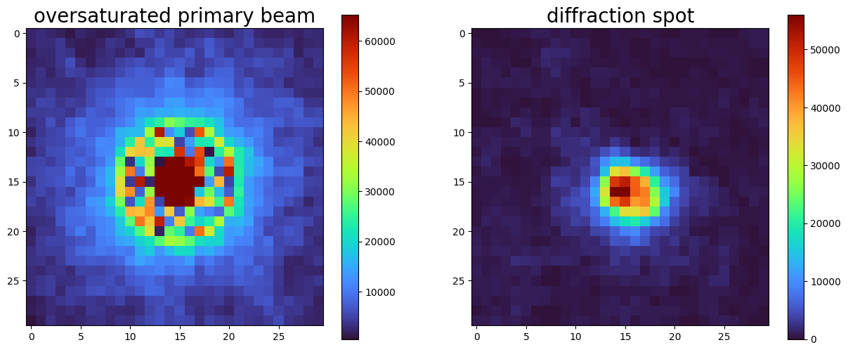
Dynamic range in one frame: exposure that saturates the primary beam (left) can still be needed to make the weakest diffraction spots (right) countable. Check both ends before starting a scan.
Practical checklist
Align the microscope and select the nanobeam aperture (often a 10–50 μm condenser aperture, or a dedicated microprobe mode).
Check the probe in real space (size, shape) and the diffraction pattern (disk sharpness) before starting a scan.
Set camera length so all reflections of interest fall on the detector; check the corners, not just the center.
Verify counts: no saturation in the central beam, adequate signal in the weakest disks you need.
Acquire calibration data: a vacuum probe image (for disk-template methods), a known calibration standard (e.g., gold nanoparticles) for pixel size and elliptical distortion, and a scan-rotation calibration.
Record all metadata (accelerating voltage, camera length, convergence angle, dwell time, probe current); your future self doing the analysis will thank you.
- Ophus, C. (2019). Four-Dimensional Scanning Transmission Electron Microscopy (4D-STEM): From Scanning Nanodiffraction to Ptychography and Beyond. Microscopy and Microanalysis, 25(3), 563–582. 10.1017/s1431927619000497
- Bustillo, K. C., Zeltmann, S. E., Chen, M., Donohue, J., Ciston, J., Ophus, C., & Minor, A. M. (2021). 4D-STEM of Beam-Sensitive Materials. Accounts of Chemical Research, 54(11), 2543–2551. 10.1021/acs.accounts.1c00073
- Nord, M., Webster, R. W. H., Paton, K. A., McVitie, S., McGrouther, D., MacLaren, I., & Paterson, G. W. (2020). Fast Pixelated Detectors in Scanning Transmission Electron Microscopy. Part I: Data Acquisition, Live Processing, and Storage. Microscopy and Microanalysis, 26(4), 653–666. 10.1017/s1431927620001713
- Tate, M. W., Purohit, P., Chamberlain, D., Nguyen, K. X., Hovden, R., Chang, C. S., Deb, P., Turgut, E., Heron, J. T., Schlom, D. G., Ralph, D. C., Fuchs, G. D., Shanks, K. S., Philipp, H. T., Muller, D. A., & Gruner, S. M. (2016). High Dynamic Range Pixel Array Detector for Scanning Transmission Electron Microscopy. Microscopy and Microanalysis, 22(1), 237–249. 10.1017/s1431927615015664