Semicrystalline polymers and small-molecule organic films (conjugated polymers for organic electronics, polyolefins, peptide and protein assemblies) derive their properties from nanoscale crystalline domains embedded in an amorphous matrix. Charge transport in an organic semiconductor, for example, depends on how the π-stacking direction of crystallites connects across the film. These materials are essentially impossible to characterize by conventional high-resolution imaging: they are extremely beam sensitive, with critical fluences of order 1–100 e⁻/Ų, destroyed long before an atomic-resolution image can be formed Bustillo et al. (2021).
Nanobeam 4D-STEM sidesteps this. Diffraction concentrates the structural information from the whole illuminated volume into a few sharp features, so a useful diffraction pattern can be recorded with orders of magnitude fewer electrons than an image Panova et al. (2016), and with a fast camera, the dose is spread over the full field of view in a single low-fluence pass.
From diffraction patterns to orientation maps
Polymer crystallites typically produce a strong, characteristic reflection (e.g., the ~3.6 Å π–π stacking peak in P3HT, or lamellar/backbone reflections at lower angles). Because of local disorder, these appear as azimuthal arcs rather than sharp spots:
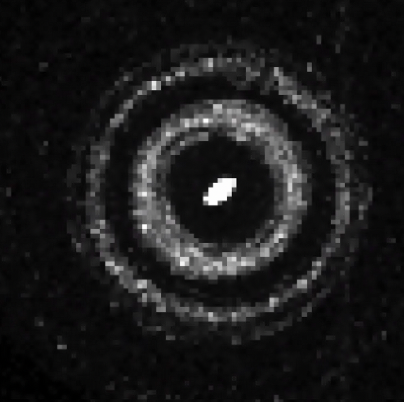
A single nanobeam pattern from a semicrystalline polymer: the characteristic reflections appear as azimuthal arcs whose angular position encodes the local crystallite orientation.
The workflow:
Detect the arcs. At each probe position, locate the azimuthal position of the characteristic reflection. Polar transformation of each pattern makes the azimuthal intensity distribution easy to fit, and peak prominence (rather than absolute intensity) is the robust detection criterion for weak, diffuse signal.
Map orientation. The azimuthal angle of the arc gives the local crystallite orientation (modulo the symmetry of the reflection); its intensity gives the degree of crystallinity/alignment. The result is an orientation field over the scanned area.
Draw flowlines. Orientation fields are hard to read as color maps alone. Flowline maps Panova et al. (2019), streamlines integrated through the orientation vector field drawn with density proportional to local alignment, render the connectivity of the crystalline regions directly, in images reminiscent of van Gogh’s Starry Night:
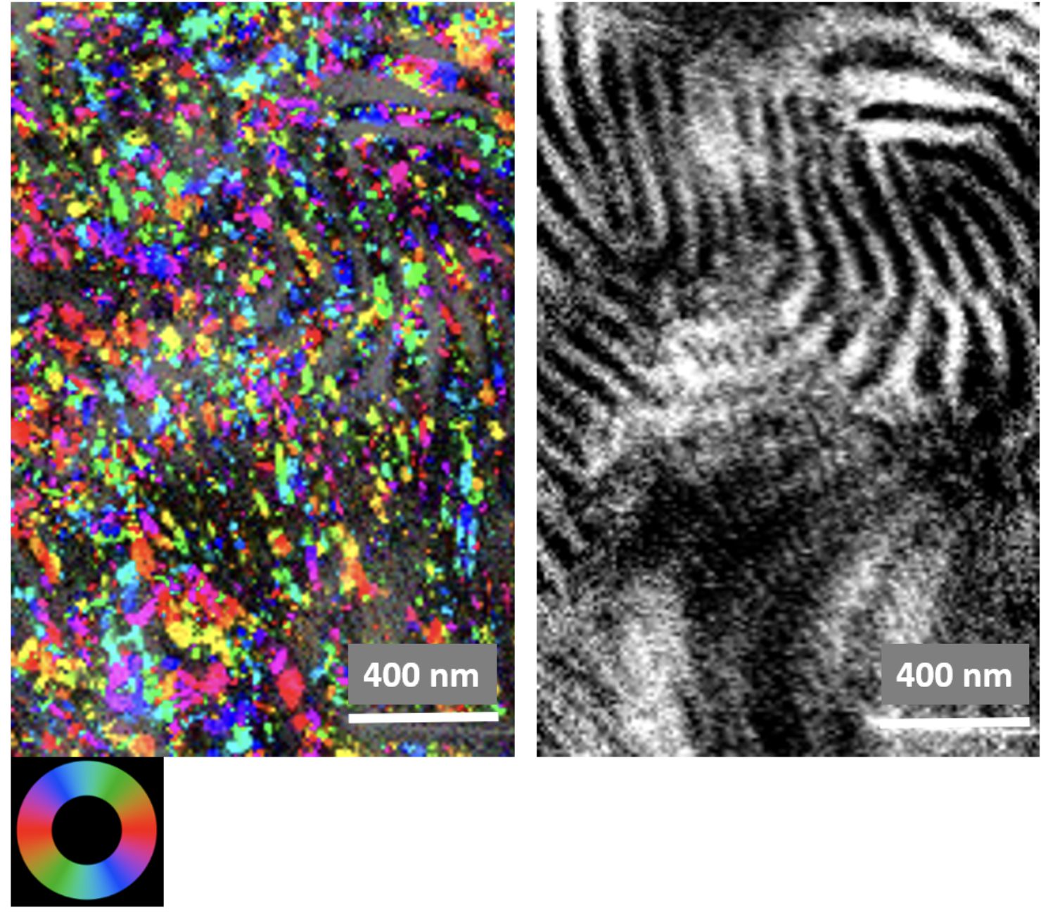
From orientation field to flowlines: the same region shown as an orientation color map (left) and as a flowline map (right). Connectivity, domain size, and topological defects in the orientation field become immediately readable.
Dose-limited experiment design
Everything about these experiments is a dose budget negotiation:
Total fluence must stay below the damage threshold; measure the critical dose for your material first (e.g., by watching a reflection fade under repeated exposure).
Step size vs. probe size: large scan steps (often ≫ probe size) spread the dose; the orientation field is smooth enough that sparse sampling still captures it.
Cryo helps: cooling typically increases critical dose by a factor of a few.
Detector: electron counting and high frame rates let you work at the shot-noise limit; pattern-level denoising and radial-symmetry priors can be applied in analysis.
- Bustillo, K. C., Zeltmann, S. E., Chen, M., Donohue, J., Ciston, J., Ophus, C., & Minor, A. M. (2021). 4D-STEM of Beam-Sensitive Materials. Accounts of Chemical Research, 54(11), 2543–2551. 10.1021/acs.accounts.1c00073
- Panova, O., Chen, X. C., Bustillo, K. C., Ophus, C., Bhatt, M. P., Balsara, N., & Minor, A. M. (2016). Orientation mapping of semicrystalline polymers using scanning electron nanobeam diffraction. Micron, 88, 30–36. 10.1016/j.micron.2016.05.008
- Panova, O., Ophus, C., Takacs, C. J., Bustillo, K. C., Balhorn, L., Salleo, A., Balsara, N., & Minor, A. M. (2019). Diffraction imaging of nanocrystalline structures in organic semiconductor molecular thin films. Nature Materials, 18(8), 860–865. 10.1038/s41563-019-0387-3