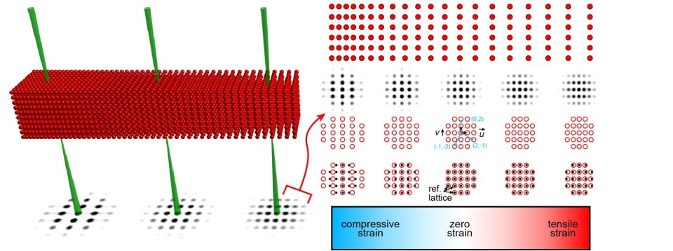
Strain, the local deviation of the lattice from its relaxed spacing, controls band structure in semiconductor devices, mobility in strained channels, ferroelastic domain patterns, and mechanical response around defects and precipitates. Nanobeam electron diffraction (NBED) strain mapping Ozdol et al. (2015) measures it directly: the positions of the Bragg disks in each diffraction pattern encode the local reciprocal lattice vectors, so tracking how disk positions shift as the probe scans across the sample gives the full 2D strain tensor (εxx, εyy, εxy, and lattice rotation θ) at every probe position, over fields of view of microns with nanometer resolution. Among the many strain-measurement techniques in the TEM Béché et al. (2013), including geometric phase analysis of high-resolution images Hÿtch et al. (1998), NBED stands out for combining large fields of view, high precision, and modest dose.
How it works
Probe template. Record a vacuum probe image (or extract a template from a thin region of the dataset). Its cross-correlation kernel, typically shaped with a sigmoid edge, is what makes disk detection precise.
Bragg disk detection. Cross-correlate the template with every diffraction pattern and locate the correlation maxima with subpixel precision Pekin et al. (2017). The key hyperparameters are the correlation power, minimum peak intensity/spacing, and the subpixel mode (
'poly'is fast for tutorials;'multicorr'is recommended for high-precision strain mapping). Always tune the detection parameters on a handful of test patterns before running the full scan.Calibration. Correct the origin (descan), elliptical distortion, and the real-space/reciprocal-space rotation; see the data handling module. Calibration errors map directly into artificial strain.
Lattice fitting. Choose basis vectors g₁ and g₂ from the Bragg vector map (ideally perpendicular, well-separated reflections), and fit the full lattice at every probe position.
Strain from a reference. Strain is always measured relative to a reference lattice: either the median lattice over a region of interest known to be unstrained, or manually specified reference vectors. The transformation between the local and reference lattice vectors, rotated into your chosen coordinate system, gives εxx, εyy, εxy, and θ.
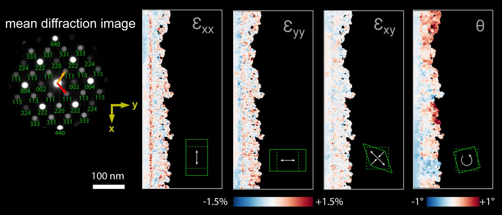
A complete result: the mean diffraction pattern with the fitted reciprocal lattice, and the four strain-tensor component maps (εxx, εyy, εxy, θ) across a multilayer structure.
Precision and pitfalls
Disk registration precision improves with sharp, uniform disk edges; this is where convergence angle, sample thickness (dynamical contrast inside the disks), and patterned probes matter. Precision of ~10⁻⁴ relative strain is achievable in favorable cases; a few ×10⁻³ is routine.
Thickness and mistilt vary across real samples and modulate the intensity inside disks, which can bias center-fitting; robust registration algorithms and (where available) precession Midgley & Eggeman (2015) help. Precession-assisted acquisition markedly narrows the strain error distribution.
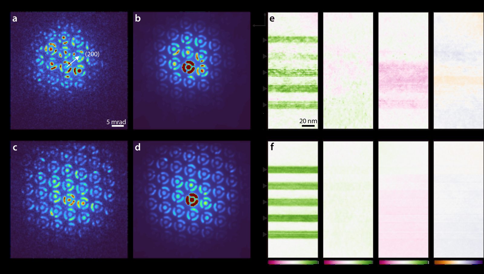
Conventional (top) vs. precession/multi-beam-averaged (bottom) acquisition of the same region: averaging through the rocking condition suppresses the dynamical intensity variations inside the disks, and the strain maps get visibly cleaner.
Patterned “bullseye” probes (apertures with concentric rings or radial spokes milled into the condenser aperture) imprint sharp internal structure onto every Bragg disk, improving registration precision severalfold at fixed dose Zeltmann et al. (2020):
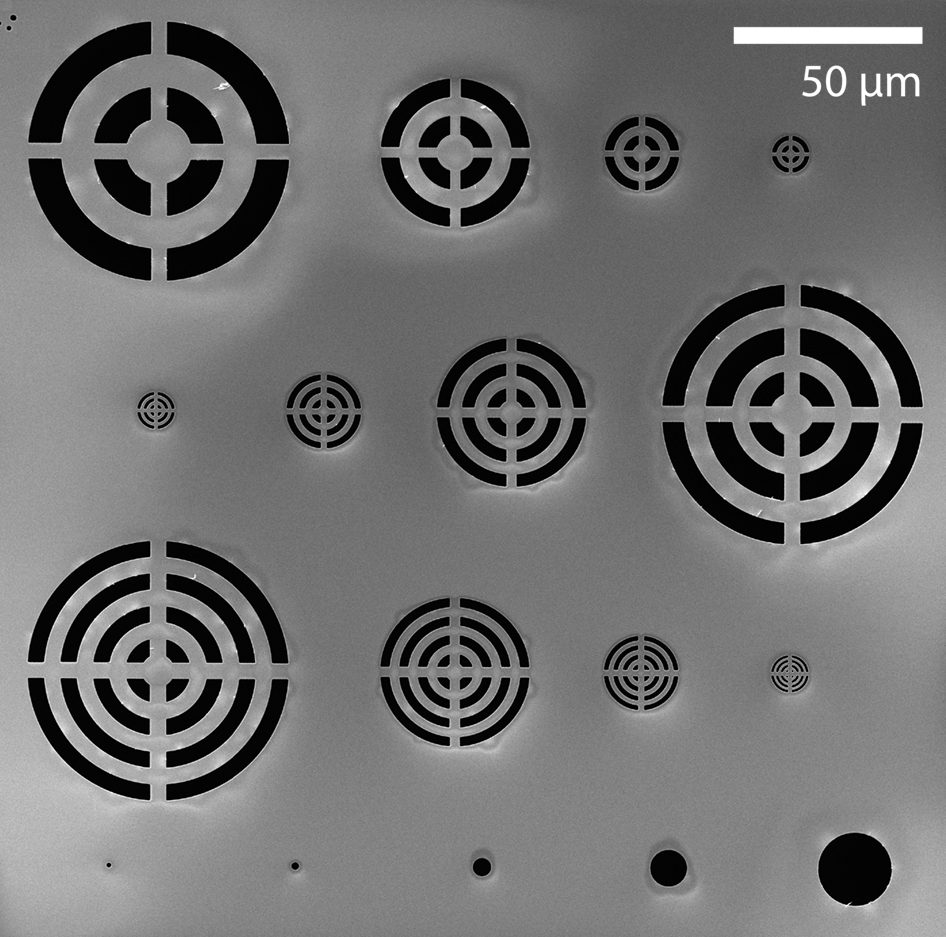
Bullseye and patterned condenser apertures fabricated with a focused ion beam. Installed in the condenser system, they shape every diffraction disk into a self-registering target.
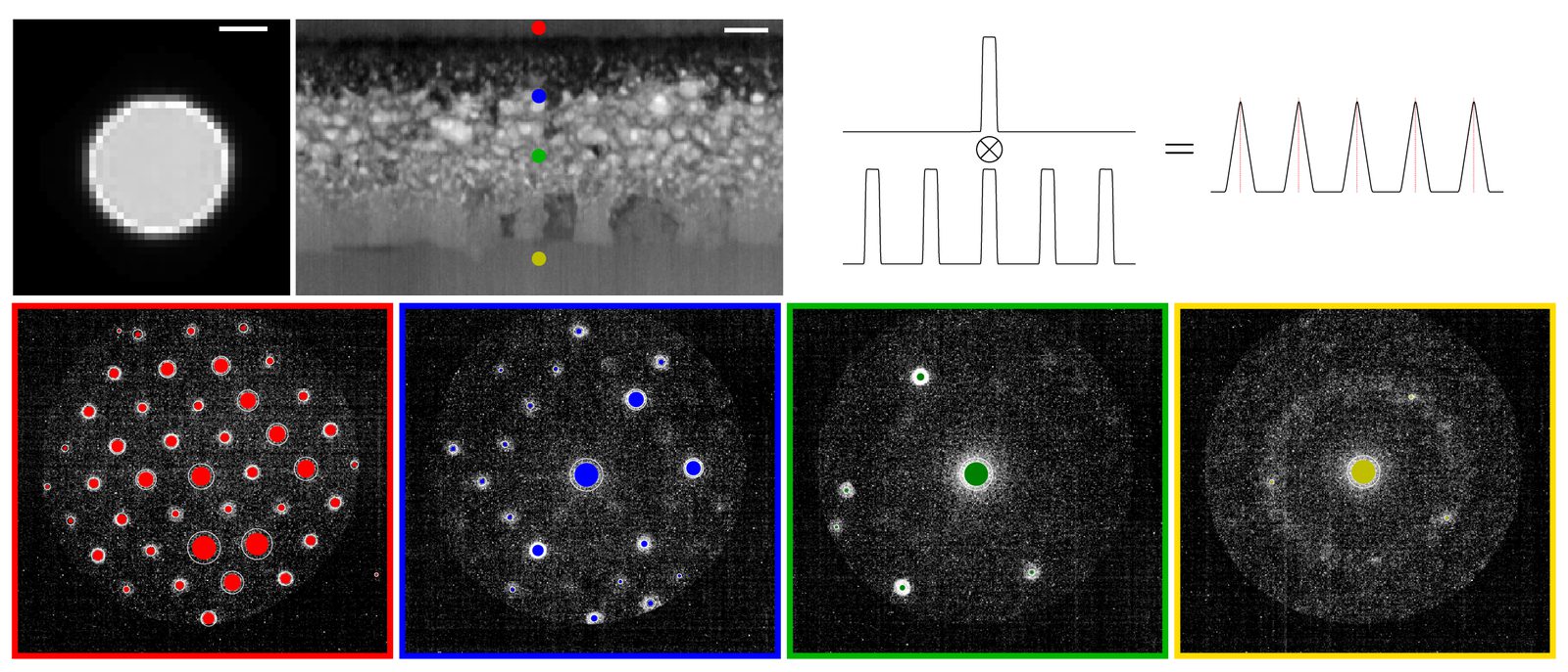
Disk detection with a bullseye probe: the patterned template cross-correlates sharply against each reflection, even where diffraction contrast varies across the disk.
The choice of reference region is a physics decision, not a software one: strain maps are only as meaningful as the reference lattice they are measured against.
Useful derived quantities: the strain dilation εxx + εyy (volumetric part), and statistics of strain over segmented regions, for example comparing precipitates against the surrounding matrix in irradiated alloys Ma et al. (2025).
- Ozdol, V. B., Gammer, C., Jin, X. G., Ercius, P., Ophus, C., Ciston, J., & Minor, A. M. (2015). Strain mapping at nanometer resolution using advanced nano-beam electron diffraction. Applied Physics Letters, 106(25). 10.1063/1.4922994
- Béché, A., Rouvière, J. L., Barnes, J. P., & Cooper, D. (2013). Strain measurement at the nanoscale: Comparison between convergent beam electron diffraction, nano-beam electron diffraction, high resolution imaging and dark field electron holography. Ultramicroscopy, 131, 10–23. 10.1016/j.ultramic.2013.03.014
- Hÿtch, M. J., Snoeck, E., & Kilaas, R. (1998). Quantitative measurement of displacement and strain fields from HREM micrographs. Ultramicroscopy, 74(3), 131–146. 10.1016/s0304-3991(98)00035-7
- Pekin, T. C., Gammer, C., Ciston, J., Minor, A. M., & Ophus, C. (2017). Optimizing disk registration algorithms for nanobeam electron diffraction strain mapping. Ultramicroscopy, 176, 170–176. 10.1016/j.ultramic.2016.12.021
- Midgley, P. A., & Eggeman, A. S. (2015). Precession electron diffraction – a topical review. IUCrJ, 2(1), 126–136. 10.1107/s2052252514022283
- Zeltmann, S. E., Müller, A., Bustillo, K. C., Savitzky, B., Hughes, L., Minor, A. M., & Ophus, C. (2020). Patterned probes for high precision 4D-STEM bragg measurements. Ultramicroscopy, 209, 112890. 10.1016/j.ultramic.2019.112890
- Ma, K., Ferreirós, P. A., Pfeifer, T. W., Abernethy, R. G., von Tiedemann, S., Peng, N., Greaves, G., Ophus, C., Sun, K., Mir, A. H., Wang, L., Huang, S., Zhao, S., Hopkins, P. E., Hardie, C. D., & Knowles, A. J. (2025). Intermetallic dispersion-strengthened ferritic superalloys with exceptional resistance to radiation-induced hardening. Acta Materialia, 293, 121095. 10.1016/j.actamat.2025.121095