

This page covers two SEM-platform techniques that extend the microscope far beyond imaging: electron backscatter diffraction, which maps crystal orientation grain by grain, and the focused ion beam, which machines site-specific cross-sections and prepares the specimens on which the rest of this course’s microscopy depends.
Electron backscatter diffraction
Tilt a polished sample to 70 degrees and place a phosphor screen with a camera a few centimeters away. Backscattered electrons diffract off lattice planes on their way out of the crystal, and because they exit traveling in essentially all directions, each set of planes Bragg-reflects some of them into a pair of shallow cones. Where these cones intersect the flat screen they appear as nearly straight bright bands (Kikuchi bands): each band is the projection of one lattice plane, its centerline the trace of the plane itself, and its angular width twice the Bragg angle, so wider bands correspond to wider-spaced planes. The pattern is therefore a gnomonic projection of the crystal’s plane geometry, a direct image of the local orientation. The steep specimen tilt exists to shallow the electron paths so that the diffracted electrons escape before losing the energy coherence the pattern needs.
Indexing is automated: the software detects the bands (via a Hough transform, which turns bands into peaks), measures the interband angles, matches them against the candidate crystal structure, and returns the orientation, all in well under a millisecond on modern systems. Scanning the beam then produces an orientation map: crystal orientation at every pixel, from which follow grain size distributions measured properly (a grain defined as a region enclosed by boundaries above a chosen misorientation angle, not estimated from image contrast), grain-boundary character including the twin fractions that dominate many FCC films, local texture that complements the ensemble pole figure, phase maps distinguishing polymorphs by their differing band geometry, and plastic strain estimates from within-grain orientation gradients (kernel average misorientation), which map stored dislocation content. Orientations are conventionally stored as Euler angles or quaternions; what matters practically is the misorientation across each boundary, the quantity that classifies boundaries (low angle versus high angle, twin versus general).
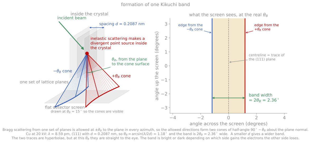
Inelastic scattering makes a divergent source inside the crystal, one plane set diffracts into two cones at , and the cones cut the flat screen as the two edges of a band of width .
For thin films, EBSD is the grain-by-grain complement to the ensemble texture measurement of XRD: XRD texture measurements give the fraction of the film in each orientation; EBSD gives the orientation of each individual grain, its size, and its neighbors. The diffracted signal originates in roughly the top 10 to 40 nm of the sample, so EBSD is a near-surface probe of crystallography rather than a surface technique in the chemical sense, and it is unforgiving of surface preparation: a few nanometers of polishing damage or oxide blurs the patterns. The practical demands are therefore a flat, damage-free, conductive surface and a crystal structure known well enough to index. Spatial resolution of roughly 20 to 50 nm bounds standard EBSD to films with grains above that scale; transmission Kikuchi diffraction (TKD), which runs the same detector with an electron-transparent sample so the patterns form in transmission from a much smaller volume, pushes resolution below 10 nm for nanocrystalline films at the cost of TEM-style sample preparation.
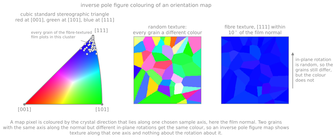
The cubic standard triangle and what its colors mean on a map. A fibre-textured film collapses to one color because one axis is fixed along the normal, while the in-plane rotation the color cannot show is still random.
The focused ion beam
A focused ion beam (FIB) instrument is an SEM whose second column focuses ions to a nanometer-scale spot. The standard source is a gallium liquid metal ion source: liquid Ga wets a tungsten needle, and the extraction field pulls the liquid into a sharp Taylor cone whose apex field-evaporates Ga ions (the same field physics as the atom probe, run as a steady source). Accelerated to 30 kV and focused to a few nanometers, the beam sputters with nanometer placement: the FIB is a milling machine at the microstructure scale, and in the dual-beam configuration the SEM column images while the ion column machines, which is what makes controlled nanofabrication routine.
Two beam-chemistry capabilities complete the toolkit. Gas-injection deposition feeds an organometallic precursor gas (commonly a platinum or tungsten compound) over the surface, where the beam decomposes it locally, writing protective straps and electrical connections; the deposit is a metal-carbon composite, conductive but far from pure. And because sputtering is directional, tilting and rocking control sidewall angles and surface finish.
The defining application for this course is the site-specific cross-section: choose any feature on a wafer, protect it with a deposited strap, mill a staircase trench beside it, and the SEM images the exposed cross-section minutes later. Extending the same operations produces the lift-out lamella for TEM: protect, mill trenches on both sides, undercut, weld the freed slab to a micromanipulator needle, transfer it to a grid, and thin it with progressively finer beams until electron transparent. The same workflow sharpened into an annular milling pattern produces the needle specimens atom probe tomography requires. Essentially every STEM image and APT reconstruction of a buried interface in the modern literature passed through this workflow, and FIB skills are now fundamental to modern microscopy.
FIB damage is the standing caveat, and it is exactly the ion-solid physics of Module 3 applied to your specimen. The 30 kV Ga beam implants gallium and amorphizes a surface layer tens of nanometers thick in silicon (of order 20 nm per exposed side), enough to dominate a thin lamella entirely if left in place; the remedy is final polishing at progressively lower voltage (5 kV, then 2 kV or below), which shrinks the damage layer to a few nanometers, mandatory practice for quantitative STEM. Redeposition of sputtered material coats nearby surfaces during aggressive milling, and curtaining, uneven milling below regions of varying density or topography, streaks cross-sections unless the surface is smoothed by a deposited strap or the geometry is rocked. Gallium itself is chemically active in some systems (it famously embrittles aluminum grain boundaries), one motivation for the xenon plasma FIB, which trades some focusability for an inert species and removal rates orders of magnitude higher, opening serial-sectioning tomography and large cross-sections of packages and solder joints. At the other extreme, the helium ion microscope focuses a gas-field-ionization He beam to sub-nanometer spots for imaging and low-damage milling. For beam-sensitive and hydrated materials, the entire workflow moves to cryogenic temperature (cryo-FIB), an approach imported from structural biology that is increasingly important for batteries and soft materials.
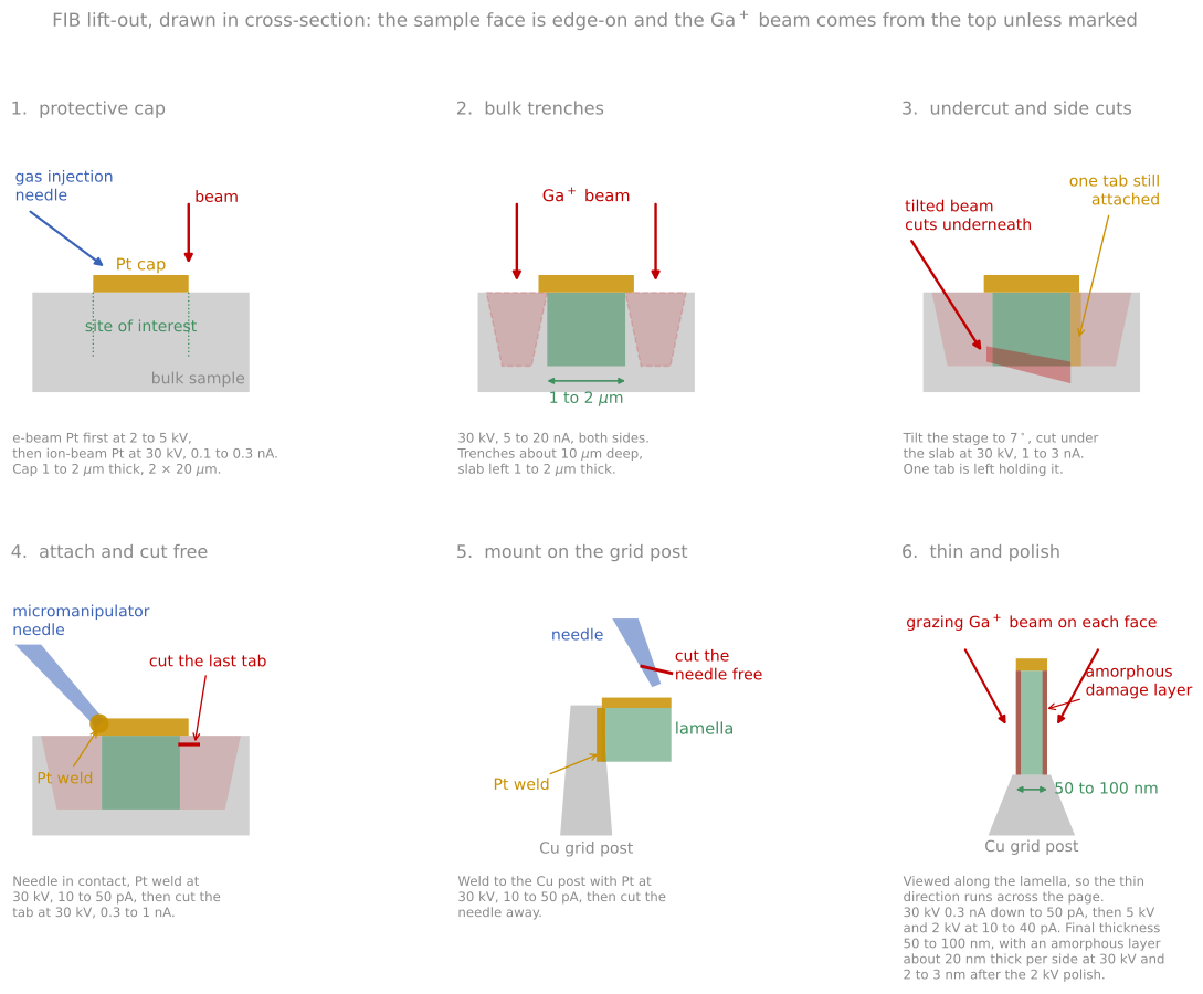
The lift-out sequence, with a representative voltage and current at each stage and the final thinning that sets both the thickness and the amorphous damage layer.
References and further reading
A. J. Schwartz, M. Kumar, B. L. Adams, and D. P. Field (eds.), Electron Backscatter Diffraction in Materials Science, 2nd ed., Springer (2009).
L. A. Giannuzzi and F. A. Stevie (eds.), Introduction to Focused Ion Beams, Springer (2005).
J. Mayer, L. A. Giannuzzi, T. Kamino, and J. Michael, TEM sample preparation and FIB-induced damage, MRS Bulletin 32, 400 (2007). Mayer et al. (2007)
- Mayer, J., Giannuzzi, L. A., Kamino, T., & Michael, J. (2007). TEM Sample Preparation and FIB-Induced Damage. MRS Bulletin, 32(5), 400–407. 10.1557/mrs2007.63