

Electrons diffract, and their diffraction is the most direct measurement of surface crystal structure we have. This page covers the two surface electron diffraction techniques: low-energy electron diffraction (LEED), the classical probe of surface crystallography, and reflection high-energy electron diffraction (RHEED), the real-time growth monitor built into nearly every MBE and oxide deposition system. Both reuse machinery from earlier modules: the reciprocal-space concepts of XRD, applied to a two-dimensional lattice, and the escape-depth physics that makes low-energy electrons surface sensitive. Both also set up the transmission diffraction of the STEM pages that follow.
Two-dimensional crystallography
A surface is periodic in two dimensions only. Its lattice is one of just five two-dimensional Bravais nets (square, rectangular, centered rectangular, hexagonal, oblique), and surface structures are named by how their mesh relates to the underlying substrate net. Wood’s notation writes the ratio of the two meshes and any rotation, Si(111) 7x7 for the famous reconstruction, c(2x2) for a centered overlayer on a square net; structures incommensurate or awkwardly related to the substrate get the more general matrix notation. Overlayers usually nucleate in several symmetry-equivalent orientations at once, and a diffraction pattern averages over these domains, a fact that must be remembered before reading symmetry off a pattern: a surface covered in equal populations of two mirror-image domains shows the combined symmetry of both.
Because the surface has no periodicity along its normal, its reciprocal “lattice” is a set of rods perpendicular to the surface rather than points: there is no third Laue condition to satisfy, and diffracted beams appear wherever the Ewald sphere crosses a rod, at every incident energy. This one geometric fact shapes everything on this page. Any periodicity larger than the substrate’s produces additional, more closely spaced rods, so reconstructions and ordered adsorbates appear as extra (fractional-order) spots.
Ewald construction for LEED and RHEED
The construction below makes the geometry explicit. In LEED mode the Ewald circle crosses the rods steeply at every energy, so diffraction never turns off, and raising the energy shrinks the pattern by pulling more rods inside the circle. Switch to RHEED mode and the enormous circle grazes the rods at a shallow angle: the highlighted chords, where the circle passes through rods of finite width, stretch into the streaks of a real RHEED pattern. The rod width is set by the inverse of the ordered domain size, so sharper crystals give sharper features in both geometries. Finally, toggle to a 3D crystal and watch the beams vanish: with reciprocal points instead of rods, an arbitrary energy and angle intersects almost nothing, which is why bulk diffraction requires scanning the angle.
LEED
LEED fires electrons of 20 to 500 eV at normal incidence and displays the elastically backscattered beams on a hemispherical fluorescent screen; a set of retarding grids in front of the screen rejects the inelastically scattered majority, passing only electrons that kept their energy and hence their diffraction information. At these energies the electron wavelength (, about 1 Å at 150 eV) matches atomic spacings and the IMFP sits at its minimum, so the pattern comes from the top few atomic layers: LEED is the surface counterpart of a single-crystal X-ray photograph.
Reading the pattern is immediate: the spot geometry gives the surface mesh and its symmetry, fractional-order spots reveal reconstructions or ordered adsorbate overlayers, and spot sharpness measures the ordered domain size, since finite domains broaden the reciprocal rods exactly as in the widget above. Diffuse background tracks disorder; spot splitting reveals regular step arrays on vicinal surfaces. A sharp, low-background pattern is the accepted certificate of a clean, well-ordered surface, which is why a LEED image opens so many surface science papers, and why a LEED optic is bolted to most UHV analysis chambers as the everyday check between preparation and measurement. Instruments optimized for lineshape analysis (spot-profile-analysis LEED) turn the broadening itself into quantitative statistics of terrace widths and step heights.
Two caveats define the technique’s scope. It requires UHV and a conductive, ordered surface. And spot positions give only the mesh, not where atoms sit within it: extracting atomic coordinates requires measuring spot intensities as a function of energy (I-V curves) and comparing them against full multiple-scattering calculations, because at these energies electrons scatter far too strongly for the single-scattering approximation to hold. This dynamical LEED analysis, iterating trial structures until calculated and measured I-V curves agree, is how the classic surface structures (including Si(111) 7x7) were confirmed quantitatively; it remains a specialist technique, and for this course the working knowledge is the pattern-level reading above.
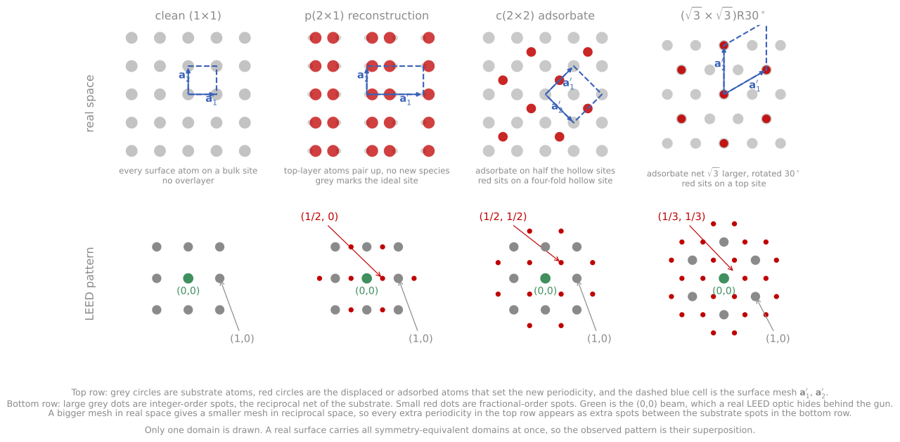
Four surface structures in real space (top) and the LEED patterns they give (bottom). Large gray spots come from the substrate mesh, small red spots are the fractional-order spots of the superstructure, and green marks the (00) beam. A larger mesh in real space gives more closely spaced spots.
RHEED
RHEED sends 10 to 30 keV electrons at grazing incidence, one to three degrees, onto the surface. The high energy would probe deeply at normal incidence, but the grazing geometry restores surface sensitivity: at grazing angles the beam’s path through the material stays within the top few atomic layers. The diffraction pattern appears on a phosphor screen across the chamber, and its geometry follows from the widget above: the Ewald sphere of a 30 keV electron ( Å) is enormous compared to the rod spacing, so it grazes along the rods, and the intersections fall on a series of circles on the screen (the Laue zones), with the zeroth zone closest to the shadow edge of the sample itself. Streaks rather than points appear whenever the rods have finite width, from finite terraces, mosaic, or disorder, because the near-tangent sphere then intersects a long segment of each broadened rod. A perfectly flat surface gives spots on the Laue circles; the long streaks of most real RHEED patterns come from surface disorder, and their length carries information about it.
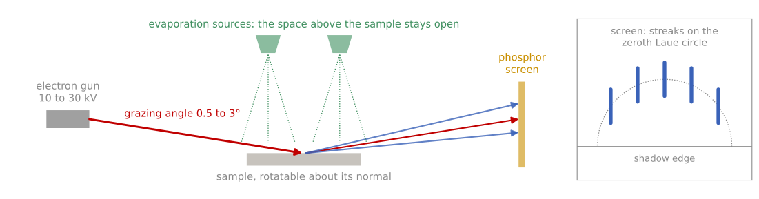
RHEED in a growth chamber, angles exaggerated. A 10 to 30 kV beam strikes the sample at a grazing angle, the reflected and diffracted beams (red and blue) reach a phosphor screen across the chamber, and the evaporation sources above the sample keep a clear path. Inset: a flat surface gives streaks along the zeroth Laue circle above the shadow edge of the sample.
The grazing geometry leaves the space above the sample completely open, which is the point: RHEED coexists with deposition sources aimed at the surface, and monitors the film as it grows. Three readings make it the growth technique it is:
Pattern character: streaks on Laue circles indicate a smooth two-dimensional surface; a spotty, transmission-like pattern means the beam is passing through three-dimensional islands, indicating roughening or island growth in real time; rings mean polycrystal; extra streak sets reveal surface reconstructions, whose appearance and disappearance calibrate temperature and flux conditions in MBE practice.
Azimuthal information: rotating the sample swings different in-plane directions through the beam, mapping in-plane symmetry and epitaxial alignment.
Intensity oscillations: in layer-by-layer growth the specular intensity oscillates with exactly one period per monolayer, as the surface cycles between smooth (complete layer, high reflectivity) and maximally stepped (half layer, low reflectivity). Counting oscillations counts monolayers, giving absolute growth-rate calibration to a fraction of a monolayer, the standard by which MBE shutters are timed. The oscillations damp as growth front roughness accumulates over multiple layers, recover during growth interruptions as the surface smooths, and vanish entirely in step-flow growth at high temperature, where atoms reach step edges before nucleating new islands, so the oscillation amplitude is itself a report on the growth mode and the surface diffusion behind it, connecting back to the Ehrlich-Schwoebel discussion of Module 1.
RHEED oscillation simulation
The simulation below grows a film one atom at a time while computing the kinematic specular intensity. With ample surface diffusion, the film completes each layer before starting the next and the intensity oscillates, one period per monolayer: this is the oscillation an MBE operator counts to calibrate growth. Drag the diffusion slider to zero and the same deposition flux produces a roughening surface and dying oscillations. The damping of real RHEED oscillations is exactly this physics, and reads as a live report on the growth mode.
References and further reading
K. Oura et al., Surface Science: An Introduction, Springer (2003), Chapters 4 and 5. The 2D crystallography and LEED treatment followed here.
A. Ichimiya and P. I. Cohen, Reflection High-Energy Electron Diffraction, Cambridge University Press (2004).
M. A. Van Hove, W. H. Weinberg, and C.-M. Chan, Low-Energy Electron Diffraction, Springer (1986). Dynamical I-V analysis.